- 您现在的位置:买卖IC网 > Sheet目录2040 > PI74ST1G125TEX (Pericom)IC BUFF TRI-ST HI SPEED SOT23-5
1
PS8521I
12/02/09
OE
GND
VCC
YOUT
AIN
1
2
4
5
3
SOTiny Gate ST
Buffer with 3-State Output
Features
High-speed: tPD = 1.8ns typical
Broad operating range: VCC = 1.8V – 3.6V
Power down high-impedance inputs/outputs
High output drive: ±24mA at 3V VCC
Packaging (Pb-free & Green available):
— 5-pin SC70 (C)
Description
The PI74ST1G125 is a buffer with 3-state output that operates over
the 1.8V to 3.6V VCC operating range.
PI74ST1G125
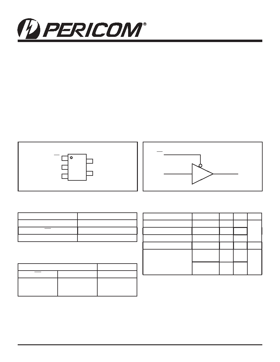
Block Diagram
Pin Conguration
OE
AIN
YOUT
Recommended Operating Conditions(1)
Parameter
Condition
Min.
Max. Units
Supply Voltage (VCC)
1.8
3.6
V
Input Voltage (VIN)
0
5.5
Output Voltage (VOUT)0
VCC
Operating Temperature
-40
85
C
Input Rise and Fall
Time (tr, tf)
VCC = 1.8V,
2.5V ±0.2V
020
ns/V
VCC = 3.3V
±0.3V
010
Notes:
1.
Unused inputs must be held HIGH or LOW. They may not oat.
Function Table (1)
Inputs
Outputs
OE
AIN
YOUT
L
H
L
H
X
L
H
X
Notes:
H = HIGH Logic Level
L = LOW Logic Level
X = Don’t Care
Z = HIGH Impedance State
Pin Description
Pin Name
Description
AIN
Input
OE
Input
YOUT
Output
09-0007
发布紧急采购,3分钟左右您将得到回复。
相关PDF资料
PI74ST1G126CEX
IC BUFF TRI-ST HIGH SPEED SC70-5
PI74STX1G126TEX
IC BUFF TRI-ST HI SPEED SOT23-5
PI74STX2G4245ZEEX
IC 2BIT LVL SHFT BUF/TXRX 12TDFN
PI74VCX16244AEX
IC BUFF/DVR 3ST 16BIT 48TSSOP
PI74VCX16245AEX
IC TXRX 16BIT BIDIR 3ST 48TSSOP
PI74VCX16373AEX
IC 16BIT D TRANSP LATCH 48TSSOP
PK-12N40PEQ
BUZZER 3-15VDC 83DB PCB 4.1KHZ
PK-12N40PQ
BUZZER PIEZO 4.1KHZ 14MM PC MT
相关代理商/技术参数
PI74ST1G125TX
制造商:Pericom Semiconductor Corporation 功能描述:Buffer/Line Driver 1-CH Non-Inverting 3-ST CMOS 5-Pin SOT-23 T/R
PI74ST1G126CEX
功能描述:缓冲器和线路驱动器 Buffer w/ TriState Output RoHS:否 制造商:Micrel 输入线路数量:1 输出线路数量:2 极性:Non-Inverting 电源电压-最大:+/- 5.5 V 电源电压-最小:+/- 2.37 V 最大工作温度:+ 85 C 安装风格:SMD/SMT 封装 / 箱体:MSOP-8 封装:Reel
PI74ST1G32CEX
功能描述:逻辑门 2 Input or Gate RoHS:否 制造商:Texas Instruments 产品:OR 逻辑系列:LVC 栅极数量:2 线路数量(输入/输出):2 / 1 高电平输出电流:- 16 mA 低电平输出电流:16 mA 传播延迟时间:3.8 ns 电源电压-最大:5.5 V 电源电压-最小:1.65 V 最大工作温度:+ 125 C 安装风格:SMD/SMT 封装 / 箱体:DCU-8 封装:Reel
PI74ST1G32TEX
功能描述:逻辑门 2 Input or Gate RoHS:否 制造商:Texas Instruments 产品:OR 逻辑系列:LVC 栅极数量:2 线路数量(输入/输出):2 / 1 高电平输出电流:- 16 mA 低电平输出电流:16 mA 传播延迟时间:3.8 ns 电源电压-最大:5.5 V 电源电压-最小:1.65 V 最大工作温度:+ 125 C 安装风格:SMD/SMT 封装 / 箱体:DCU-8 封装:Reel
PI74ST1G32TX
制造商:Pericom Semiconductor Corporation 功能描述:
PI74ST1G86CEX
功能描述:逻辑门 2 Input XOR Gate RoHS:否 制造商:Texas Instruments 产品:OR 逻辑系列:LVC 栅极数量:2 线路数量(输入/输出):2 / 1 高电平输出电流:- 16 mA 低电平输出电流:16 mA 传播延迟时间:3.8 ns 电源电压-最大:5.5 V 电源电压-最小:1.65 V 最大工作温度:+ 125 C 安装风格:SMD/SMT 封装 / 箱体:DCU-8 封装:Reel
PI74ST1G86CX
制造商:Pericom Semiconductor Corporation 功能描述:
PI74STX1G00CX
功能描述:IC SINGLE 2-IN NAND GATE SC70-5 RoHS:否 类别:集成电路 (IC) >> 逻辑 - 栅极和逆变器 系列:74STX 标准包装:2,000 系列:74LCX 逻辑类型:逆变器,缓冲器 电路数:1 输入数:8 特点:三态 电源电压:2 V ~ 3.6 V 电流 - 静态(最大值):10µA 输出电流高,低:24mA,24mA 逻辑电平 - 低:0.7 V ~ 0.8 V 逻辑电平 - 高:1.7 V ~ 2 V 额定电压和最大 CL 时的最大传播延迟:6.5ns @ 3.3V,50pF 工作温度:-40°C ~ 85°C 安装类型:表面贴装 供应商设备封装:20-SSOP 封装/外壳:20-SSOP(0.209",5.30mm 宽) 包装:带卷 (TR)